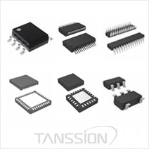
Ⅰ. Description of bipolar junction transistor
Ⅱ. The parameters of BJT
Ⅲ. The working principle of BJT
Ⅳ. The working state of BJT
Ⅴ. The characteristics of BJT
Ⅵ. The classification of BJT
Ⅶ. Bipolar junction transistor detection
Ⅰ. Description of bipolar junction transistor
Bipolar junction transistor (BJT) is also called a bipolar transistor and a transistor, and is a semiconductor device that controls current. Its function is to amplify the weak signal into an electrical signal with a larger amplitude value, and it is also used as a non-contact switch.
The bipolar junction transistor is one of the basic components of semiconductors. It has the function of current amplification and is the core component of electronic circuits. The bipolar junction transistor is made on a semiconductor substrate with two PN junctions that are very close to each other. The two PN junctions divide the whole semiconductor into three parts. The middle part is the base area, and the two sides are the emitter area and the collector area. The arrangement is PNP And NPN two kinds.

Ⅱ. The parameters of BJT
1. Reverse current between poles
The smaller the reverse current between electrodes, the higher the stability of the bipolar junction transistor.
2. Working frequency
The β value of the bipolar junction transistor remains unchanged only within a certain operating frequency range. If the frequency range is exceeded, they will drop off sharply as the frequency increases.
3. Reverse breakdown characteristics
A bipolar junction transistor is composed of two PN junctions. If the reverse voltage exceeds the rated value, it will break down like a diode, degrading its performance or permanently damaging it.
4. Beta value
The β value is the most important parameter of the bipolar junction transistor, because the β value describes the ability of the bipolar junction transistor to amplify the current signal. The higher the β value, the stronger the ability to amplify small signals, and vice versa. But the value of β cannot be too large, because too large will affect the stability of the bipolar junction transistor. Usually the β value should be in the range of 30 to 80. Generally speaking, the β value of the bipolar junction transistor is not a specific value. It generally changes slightly with the working state of the component.
Ⅲ. The working principle of BJT
1. Theoretical principles
Crystal transistors are divided into germanium tubes and silicon tubes according to their materials, and each has two structural forms, NPN and PNP, but the most commonly used are silicon NPN and PNP transistors. Both work in the same way except for the polarity of the power supply. The current amplification principle of the NPN silicon tube is introduced below.
The NPN tube is composed of two N-type semiconductors sandwiching a P-type semiconductor. The PN junction formed between the emitter region and the base region is called the emitter junction, and the PN junction formed between the collector region and the base region is called the collector junction. The three leads are called emitter e (Emitter), base b (Base) and collector c (Collector). When the potential at point b is a few tenths of a volt higher than the potential at point e, the emitter junction is in a forward biased state. When the potential at point C is several volts higher than the potential at point B, the collector junction is in a reverse biased state. The collector power supply Ec is higher than the base power supply Ebo.
When manufacturing a bipolar junction transistor, we must consciously make the majority carrier concentration in the emitter region greater than that in the base region. At the same time, the base area is made very thin, and we must strictly control the impurity content. In this way, once the power is turned on, due to the correct emitter junction, the majority carriers (holes) in the base region of the majority carrier (electron) in the emission region can easily cross the emission structure and diffuse to each other. But because the concentration of the former is greater than that of the latter, the current passing through the emitter junction is basically an electron flow, and this electron flow is called the emitter current Ie.
Due to the thinness of the base region and the reverse bias of the collector junction, most of the electrons injected into the base region cross the collector junction and enter the collector region to form a collector current Ic, leaving only a small amount (1-10%) Electrons recombine with holes in the base region. The recombined base holes are replenished by the base power supply Eb, thus forming the base current Ibo according to the current continuity principle:
Ie=Ib+Ic
That is to say, by adding a small Ib at the base, a larger Ic can be obtained at the collector, which is the so-called current amplification effect. Ic and Ib maintain a certain proportional relationship, namely:
β1=Ic/Ib
In the formula: β is called the DC magnification.
The ratio of the change in collector current △Ic to the change in base current △Ib is:
β= △Ic/△Ib
In the formula, β is called the magnification of the alternating current. Since the values of β1 and β are not much different at low frequencies, we do not make a strict distinction between the two. The value of β is about tens to more than one hundred.
2. Amplification principle
(1) The emission area emits electrons to the base area
The power supply Ub is added to the emitter junction through the resistor Rb, and the emitter junction is forward-biased. The majority carriers (free electrons) in the emitter region continuously cross the emitter junction and enter the base region, forming the emitter current le. At the same time, the majority carriers in the base region also diffuse to the emitter region. But since the majority carrier concentration is much lower than the carrier concentration in the emitter region, we can ignore this current. So we can think that the emitter junction is mainly electron flow.
(2) Diffusion and recombination of electrons in the base region
After electrons enter the base region, they are densely concentrated near the emitter junction, gradually forming a difference in electron concentration. Under the action of the concentration difference, it promotes the electron flow in the base region to diffuse to the collector junction, and is pulled into the collector region by the collector junction electric field to form the collector current lc. There is also a very small part of electrons (because the base area is very thin) recombined with the holes in the base area, and the ratio of the diffused electron flow to the recombined electron flow determines the amplification capability of the bipolar junction transistor.
(3) The collector area collects electrons
Due to the large reverse voltage applied to the collector junction, the electric field force generated by this reverse voltage will prevent the diffusion of electrons from the collector region to the base region, and at the same time, the electrons diffused near the collector junction will be pulled into the collector region to form the main current lcn of the collector. In addition, the minority carriers (holes) in the collector region will also generate drift motion, forming a reverse saturation current flowing towards the base region. It is represented by lcbo, which has a small value but is extremely sensitive to temperature.

Ⅳ. The working state of BJT
1. Amplified state
When the voltage applied to the emitter junction of the bipolar junction transistor is higher than the turn-on voltage of the PN junction and reaches a certain value, the emitter junction of the bipolar junction transistor will be forward-biased, and the collector junction will be reverse-biased. At this time, The current at the base will affect the current at the collector, which causes the bipolar junction transistor to have a current amplification effect. Its current amplification factor β=ΔIc/ΔIb, at this moment, the bipolar junction transistor is in the amplified state.
2. Cut-off state
When the voltage applied to the emitter junction of the transistor is less than the conduction voltage of the PN junction, the base current is zero, and both the collector current and emitter current are zero. At this point, the transistor loses its current amplification effect, and the disconnection state between the collector and emitter is equivalent to a switch. We call the transistor in the cut-off state.
3. Saturated conduction state
When the voltage applied to the emitter junction of the transistor is greater than the conduction voltage of the PN junction, and the base current increases to a certain extent, the collector current no longer increases with the increase of the base current, but remains unchanged near a certain value. At this point, the transistor loses its current amplification function. The voltage between the collector and emitter is very small, and the conduction state between the collector and emitter is equivalent to that of a switch. This state of the transistor is called the saturated conduction state.
Ⅴ. The characteristics of BJT
1. Amplification characteristics
A small change in the b-pole current can cause a large change in the c-pole current.
2. Flow control characteristics
That is, the current controls the current. The b-pole current can control the presence and size of the c-pole current.
3. Switching characteristics
In addition to the amplification function, the bipolar junction transistor can also be used as a switch. For example, when the e pole of the NPN bipolar junction transistor is grounded and the b pole current is >1mA, the bipolar junction transistor is completely turned on and acts as a switch.
Ⅵ. The classification of BJT
1. According to the structure
(1) NPN transistor
In NPN, there is a p-type material existing between two n-type materials. NPN transistors are basically used to amplify weak signals into strong ones. In an NPN transistor, electrons move from the emitter region to the collector region, creating a current flow in the transistor. Such transistors are widely used in circuits.
Advantages:
① When the system is first powered on, the base is a certain low level.
② When the base control level is changed from high to low, the base can be pulled down faster, and the NPN transistor can be cut off faster and more reliably.
(2) PNP transistor
A PNP is a type of BJT in which an n-type material is introduced or placed between two p-type materials. In such a configuration, the device will control the flow of electrical current. A PNP transistor consists of 2 crystal diodes connected in series. The right and left side of the diode are called collector, base diode and emitter-base diode respectively.
Advantages:
① When the system is first powered on, the base is a certain high level.
② When the base control level is changed from low to high, the base can be pulled up faster, and the PNP transistor can be cut off faster and more reliably.
2. According to the semiconductor material
(1) Silicon bipolar junction transistors
Compared with germanium bipolar junction transistors, silicon bipolar junction transistors have smaller reverse leakage currents, flat output characteristics, relatively high withstand voltage, and better temperature characteristics.
(2) Germanium bipolar junction transistors
The germanium bipolar junction transistors has a lower initial working voltage and a lower saturation voltage drop than the silicon bipolar junction transistors. When the bipolar junction transistor is turned on, the voltage of the emitter and collector is lower for the germanium bipolar junction transistors than for the silicon bipolar junction transistors. Because the forward conduction voltage of the PN junction made of germanium material is lower than that of the P junction made of silicon material. The former is 0.2~0.3W, and the latter is 0.6~0.7V. Therefore, the germanium bipolar junction transistor only has a voltage of 0.2~0.3V between the emitter and the base, and the transistor starts to work.
3. According to the function
The switch bipolar junction transistor controls the transition between the saturation region and the cut-off region. The response time of the switching process of the switching transistor. The length of the switch response time indicates the quality of the transistor switching characteristics.
It is also called composite bipolar junction transistor. It combines two bipolar junction transistors together to form an equivalent new bipolar junction transistor. The magnification of a Darlington transistor is the product of the magnifications of the two transistors. A Darlington transistor can be seen as a direct coupled amplifier. The bipolar junction transistors are directly connected in series without any coupling elements.
Advantages:
It has high magnification. We often use Darlington tubes in power amplifiers and regulated power supplies.
Disadvantages:
① Compared to general switch transistors, its output voltage drop is one more level.
② It is susceptible to interference. When designing the circuit, we should also pay attention to the relevant protection measures.
(3) Phototransistor
Compared with conventional bipolar junction transistors, phototransistors have a larger area in the base area and a smaller area in the light emitting area. A phototransistor is a device that amplifies light, electricity, and light signals. In the base region, due to the input of the optical signal, the electrons and holes in the semiconductor will move, resulting in the accumulation of holes in the emitter region, which is equivalent to adding a positive bias to the emitter, so that the phototransistor has the amplification effect. The electrical signal measured by the phototransistor will be amplified as the incident light changes. Phototransistors are widely used in optical detection, photoelectric sensing, automatic control, optical coupling, encoders, decoders and laser receiving.
4. According to power consumption
(1) Low-frequency low-power bipolar junction transistor
It refers to a bipolar junction transistor with a characteristic frequency below 3MHz and a power of less than 1W.
(2) High-frequency low-power bipolar junction transistor
It refers to a bipolar junction transistor with a characteristic frequency greater than 3MHz and a power less than 1W. It is mainly used in high-frequency oscillation and amplifier circuits.
(3) Low frequency high power bipolar junction transistor
It refers to a bipolar junction transistor with a characteristic frequency less than 3MHz and a power greater than 1W. There are many varieties of low-frequency high-power bipolar junction transistors, which are mainly used in low-frequency power amplifier circuits of electronic audio equipment.
(4) High-frequency high-power bipolar junction transistor
High-frequency high-power bipolar junction transistor refers to a bipolar junction transistor with a characteristic frequency greater than 3MHz and a power greater than 1W. It is mainly used for power drive and amplification in communication and other equipment.

Ⅶ. Bipolar junction transistor detection
Below are several methods for measuring transistors with a multimeter.
1. Determine the pins of the transistor
The three pins of the bipolar junction transistor have different functions and cannot replace each other during operation. We put the multimeter in the resistance R×1KQ range, connect the black test lead of the multimeter to a certain pin of the transistor (assuming it is the base), and connect the other two electrodes with the red test lead. If the two resistance values indicated by the needle are very small, then the pin connected to the black test lead is the base of the NPN tube. If the two resistance values indicated by the needle are very large, then the pin connected to the black test lead is the base of the PNP tube. If one of the resistance values indicated by the hands is very large and the other is very small, then the pin connected to the black test lead must not be the base of the bipolar junction transistor, and we need to change another pin to test again.
2. Judgment of silicon tube and germanium tube
We use the difference between the forward and reverse resistance of the silicon tube PN junction and the germanium tube PN junction to judge whether the bipolar junction transistor of unknown type is a silicon tube or a germanium tube. Use the R×1KQ file of the multimeter to measure the forward resistance between the emitter and the base and between the collector and the base. The silicon tube is about 3-10KQ, and the germanium tube is about 500-1KQ.
3. Measure the DC magnification of the bipolar junction transistor
We adjust the function selection switch of the multimeter to HFE and adjust it to zero, and put the three electrodes of the bipolar junction transistor into the four small holes on the panel of the multimeter correctly. e, b, c of PNP (P) or NPN (N) At this time, the pointer of the multimeter will deflect to the right. There is an indicator of HFE on the dial inside the meter head, which is the DC magnification of the measuring bipolar junction transistor.
标签:Discrete Semiconductor Transistors - Bipolar (BJT) - Single