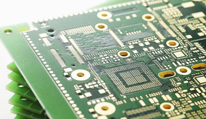
Ⅰ.Characteristics of PCB
1. High reliability
Through a series of technical means such as inspection, testing and aging test, the PCB can be guaranteed to work reliably for a long time (generally 20 years).
2. High density possible
Over the years, the high density of PCB has been able to develop correspondingly with the improvement of integrated circuit integration and the progress of mounting technology.
3. Maintainability
Since PCB products and components assembled as a whole are designed and produced in a standardized manner, these components are also standardized. Therefore, once the system fails, it can be replaced quickly, conveniently and flexibly, and the work of the system can be quickly restored.
4. Assemblability
PCB products are not only convenient for standardized assembly of various components, but also can be automated and large-scale mass production. In addition, the overall assembly of PCB and various other components can also form larger components, systems, and even the whole machine.
5. Manufacturability
PCB adopts modern management, which can realize standardization, scale (quantity) and automatic production, so as to ensure the consistency of product quality.
6. Designability
The requirements for various performances (electrical, physical, chemical, mechanical, etc.) of PCB can be achieved through standardization and standardization of design. In this way, the design time is short and the efficiency is high.
7. Testability
A relatively complete test method and test standard has been established, and various test equipment and instruments can be used to detect and identify the qualification and service life of PCB products.
8. Assemblability
PCB products are not only convenient for standardized assembly of various components, but also can be automated and large-scale mass production. In addition, the overall assembly of PCB and various other components can also form larger components, systems, and even the whole machine.
Ⅱ.Classification of PCB
1. Classified by layers:
single sided
Is one of the simplest types of printed circuit boards, it has only one conductive layer on one surface. Since there is only one conductive layer, it works well for low-frequency circuits and simple electronic applications, and is relatively simple and low-cost to design and manufacture. The single-sided board has a larger layout space, which is suitable for larger-sized electronic components and layouts.
Double panel
Is a type of printed circuit board that has conductive layers on both surfaces. Compared with single-sided PCBs, double-sided PCBs can accommodate more electronic components and connections, making them suitable for more complex electronic equipment and circuit designs. Double-sided PCB has two conductive layers, which can arrange more connections and components on the same board, thereby increasing the density of the circuit. Thanks to two conductive layers, signal traces can be distributed on two different layers, reducing interference and crosstalk.
multilayer board
It is a printed circuit board with conductive layers and interlayer insulating layers on multiple levels. Compared with single-sided and double-sided PCBs, multilayer PCBs can accommodate more layers, enabling more complex circuit designs and higher circuit densities in a smaller space. The laminate PCB can arrange signal traces and electronic components on different levels, thereby greatly increasing the circuit density and suitable for high-density wiring requirements. Different layers can be used to isolate different types of signals, reduce interference, and improve signal integrity. Multilayer PCBs can provide more complex circuit interconnections by passing signals and power between different layers through hole connections. Multilayer PCBs are suitable for handling radio frequency and high-speed digital signals because they can use different layers to manage the signals.
2. Classified by purpose:
Universal PCB
It is a relatively standardized and versatile printed circuit board, suitable for a variety of different types of electronic equipment and applications. General-purpose PCBs are usually single-sided, double-sided or multi-layer boards, from simple to complex, from low frequency to high frequency. Universal PCBs are designed and manufactured to accommodate a variety of different types of electronic equipment, from home appliances to industrial controls, consumer electronics, and communication equipment, among others. Common PCBs usually follow industry standards, such as dimensions, connection interfaces, etc., to make it easier to use in different applications.
High frequency PCB
It is a printed circuit board specially designed and manufactured for processing high frequency signals. Since high-frequency signals will exhibit special electromagnetic characteristics and transmission behavior in PCBs, more factors need to be considered in the design and manufacture of high-frequency PCBs to ensure signal stability and performance. In the high-frequency range, the transmission behavior of the signal will be affected, so high-frequency PCBs require special design and manufacture to ensure signal integrity and reduce signal loss.
High-frequency signals are easily affected by electromagnetic interference, so high-frequency PCBs require effective electromagnetic shielding and interference suppression measures. High-frequency PCBs usually use special high-frequency materials, such as PTFE (polytetrafluoroethylene), etc., to have lower dielectric constant and loss, so as to maintain signal quality. Transmission lines in high-frequency PCBs need to be strictly controlled in width, spacing, and impedance to accommodate the characteristics of high-frequency signals.
Power PCB
is a printed circuit board specially designed and manufactured to handle high power circuits. In high-power circuits, the transmission requirements of current and energy are higher, so the design and manufacture of power PCBs need to consider more factors such as heat dissipation, current carrying and insulation. Power circuits need to carry high current, so the power PCB needs to use large enough wires and connections to ensure the stability of current transmission. In high-power circuits, electronic components may generate a lot of heat, so power PCBs need to consider effective thermal management designs, such as heat sinks, heat sinks, etc.
Power circuits need to work under high load conditions, so the material and design of the power PCB need to be strong and durable enough. There may be high voltage in the power circuit, and the power PCB needs to ensure electrical isolation to prevent short circuit and electric shock.
high speed PCB
Printed circuit boards for processing high-speed digital signals. In high-speed signal transmission, factors such as signal transmission delay, signal integrity and interference suppression become particularly important. In high-speed signal transmission, signal integrity and stability become critical, requiring precise signal trace layout and control.
In high-speed digital circuits, signal transmission delay may affect the performance of the system, so high-speed PCB needs to consider control signal transmission delay. In high-speed signal transmission, cross-interference between signals may cause signal distortion, so high-speed PCBs require effective interference suppression measures. In high-speed PCBs, the impedance control of signals is very important to ensure the matching and optimal transmission of signals.
3. Classification by connection method:
Flexible PCB
It is a printed circuit board manufactured using a flexible substrate that can be bent, folded and bent to a certain extent and is suitable for electronic devices and applications that require flexibility and compactness. Flexible PCBs can be bent and folded to a certain extent, making them suitable for electronic devices that require curved surface designs.
Since flex PCBs can be bent, they can better accommodate small and compact device designs. Flexible PCBs are generally lighter than traditional rigid PCBs and are suitable for applications that require lightweighting. Due to the bendability of flex PCBs, they perform better in vibration and shock environments.
Rigid PCB
It is a printed circuit board manufactured using a rigid base material whose main feature is that it cannot be bent or folded to a certain extent. The main feature of a rigid PCB is stability, which is not prone to deformation or change, so it is suitable for applications that require stable circuit connections.
Due to the fixed structure of the rigid PCB, its circuit connection is relatively stable and can provide high reliability. Rigid PCB usually has a larger layout space, suitable for larger size electronic components and layout. The design and manufacturing process for rigid PCBs has been standardized, making mass production easier and cost-effective.
Rigid-flex PCB
It is a printed circuit board that combines the characteristics of rigid PCB and flexible PCB. This design allows both rigid and flexible parts to exist in the same PCB, thus combining the advantages of both in one design. Rigid-flex PCBs usually have multiple layers, with rigid parts for carrying electronic components and connections, and flexible parts for areas that need to be bent and folded.
By combining rigid and flexible parts, rigid-flex PCBs are able to meet both requirements in areas where flexibility and stability are required. Rigid-flex PCB can reduce assembly steps, because rigid and flexible parts can be implemented on the same PCB. It does not require the use of additional wires or connectors to connect the rigid and flexible parts.
4. Classification by manufacturing process:
Traditional PCB
Often referred to as a rigid printed circuit board, it is an electronic circuit board made of a rigid substrate used to connect and support electronic components. The main feature of traditional PCB is stability, the shape and structure of the circuit board are not easy to change, so it is suitable for applications that require stable circuit connections. Traditional PCBs can have multiple layers, allowing for more complex circuit designs and connections on one board.
Due to the relatively fixed structure of rigid PCBs, they usually provide high reliability and circuit connection stability. The process of manufacturing and designing traditional PCBs has been standardized, making mass production easier and cost-effective.
RF PCB
A printed circuit board for processing radio frequency signals. In radio frequency applications, the frequency of the signal is usually in the range of hundreds of megahertz (MHz) to several gigahertz (GHz), and there are special requirements for circuit design and manufacture to ensure signal stability, transmission performance and minimize signal loss.
In RF applications, the integrity and stability of the signal is of paramount importance, so the RF PCB needs to strictly control the signal transmission path, matching and impedance. RF signals are susceptible to loss during transmission. The design and manufacture of RF PCBs need to minimize signal loss, including wires, connectors, boards, etc.
RF signals are easily affected by electromagnetic interference, and RF PCBs need to take effective electromagnetic shielding and interference suppression measures. RF PCBs usually use special high-frequency materials, such as PTFE (polytetrafluoroethylene), etc., to have lower dielectric constant and loss, so as to maintain signal quality.
High Density Interconnect PCB
HDI PCB, referred to as HDI PCB, is a design and manufacturing method aimed at achieving more and more compact circuit connections in a limited space. HDI PCB achieves higher circuit density, smaller size and higher performance by adopting advanced design technology and manufacturing process.
HDI PCBs usually use a multi-layer design to achieve higher circuit density by stacking signal and power layers together. HDI PCB adopts blind hole and buried hole technology, which allows more complex signal transmission and connection inside the multilayer board. HDI PCB allows multiple functional components and circuits to be integrated in a small package, providing a higher level of integration.
5. Classified by special characteristics:
Impedance Control PCB
It refers to the realization of precise circuit impedance matching through specific design and manufacturing techniques during the design and manufacture of printed circuit boards (PCBs). Circuit impedance is an important parameter of signal transmission in the circuit, especially in high frequency, high speed, radio frequency and other applications, accurate impedance matching can ensure the stability and integrity of signal transmission. Through impedance control, signal reflection and loss can be reduced, thereby improving signal transmission stability.
Impedance control is especially important in applications such as high frequency, radio frequency, where the transmission characteristics of the signal are more sensitive.
Impedance control PCB is also very important in differential signal transmission, because differential signals have higher requirements for impedance matching.
Blind Buried Via PCB
It is a printed circuit board (PCB) design and manufacturing technique used to realize the connection of different layers of circuits in a multilayer PCB. This technique allows connections to internal layers through one side of the board without penetrating the entire board thickness, enabling higher circuit densities and more complex layouts. Blind and buried via technology allows more circuit connections in a limited space, improving circuit density and functionality. By reducing the length of signal lines, blind buried vias can reduce interference between signal lines.
Blind buried hole PCB is divided into buried hole and blind hole:
Buried Via: Buried Via is a hole that connects the internal layers of the PCB, completely inside the board and will not be visible from the surface of the board.
Blind Via: A blind via is a hole that connects the outer and inner layers of the PCB, and it is only visible on one side of the board. Such holes do not run through the thickness of the entire PCB board, but only connect part of the layers.
Ⅲ. What is the common method of PCB soldering?
1.Through-Hole Technology, THT: For larger components and connectors, wave soldering is often used. This involves inserting electronic components into holes in the PCB, then inserting the entire PCB into a solder surge, causing the solder to adhere to the pins and secure the components.
2.SMT, Surface Mount Technology: This is one of the most common PCB soldering methods. The pins of the electronic components are adhered to the surface of the PCB by solder paste, and then baked by hot air or heat-treated in a reflow oven to melt the solder paste and fix the components. SMT is suitable for small, high-density components, such as chip components, diodes, capacitors, etc.
3. Manual welding: For some smaller production batches or special requirements, the manual welding method may be used. This involves using a handheld soldering iron to solder the pins of electronic components.
4.Hot Bar Soldering: This is a method that uses a hot plate and hot press between two connecting parts to connect electronic components to the PCB. This is often used in the connection of tiny components or flexible electronic components.
5. Reflow soldering: In SMT, reflow soldering is the main method of soldering electronic components to PCB. It involves passing the PCB through a reflow oven or hot air to melt the solder paste and secure the components.
6.Vapor Phase Soldering: Vapor Phase Soldering is a method of completing soldering by creating saturated steam between the PCB and the components. This method provides high accuracy and uniformity in SMT applications.
Ⅳ.PCB assembly process
First, purchase the required electronic components, including chips, resistors, capacitors, connectors, etc. These components will be soldered to the PCB to build the circuit.
In the SMT stage, an automatic placement machine is used to place electronic components precisely on the designed positions on the PCB. The pick and place machine automatically recognizes the components and places them in the correct position according to the component layout and data on the PCB.
Components placed on the PCB require soldering to secure them and establish circuit connections. This is typically done by applying solder paste to the component leads, then passing the paste through a reflow oven to melt it and form a solder connection. After the solder paste has cured, the components are fixed on the PCB.
During assembly, automated optical or X-ray inspections are often performed to verify the quality and correctness of the welds. Subsequently, electrical testing and functional testing may be performed to ensure that the assembled circuit is working properly.
For components that cannot be soldered by SMT, such as connectors and large components, plug-in assembly is used.
Ⅴ. What are the impacts of PCB manufacturing and disposal on the environment?
1. Energy consumption: PCB manufacturing requires a lot of energy, including electricity and fuel. Electricity is mainly used for machinery and heating processes, while fuel is used for heating and welding processes. Energy consumption leads to carbon emissions and resource depletion.
2. Resource consumption: The manufacture of PCB requires a lot of raw materials, including metals, chemicals and water. Metals such as copper and gold are the main materials for circuit boards, and their mining and processing have environmental impacts. Chemicals such as printing inks, coatings and solvents are also consumed during the production process.
3. Waste treatment: The waste of PCB equipment includes waste electronic equipment, waste PCB boards, waste electronic components, etc. These wastes usually contain hazardous substances, such as heavy metals and dangerous chemicals, which need to be properly treated and recycled to reduce environmental pollution.
4. Emission of chemical substances: Chemical substances used in PCB manufacturing and processing may be discharged into the atmosphere, water and soil, causing environmental pollution. Some chemicals may pose environmental and health hazards.
5. Waste generation: PCB manufacturing generates a lot of waste, including waste, waste water and exhaust gas. The treatment and disposal of waste consumes resources, and improper treatment may lead to environmental pollution.
6. Water resource use: PCB manufacturing requires a lot of water for cooling, cleaning and handling chemicals, etc. Excessive use of water resources can lead to depletion or pollution of local water sources.
In order to reduce the impact of PCB on the environment, the following measures can be taken:
Adopt green manufacturing and environmentally friendly processes, use environmentally friendly materials and substitutes; choose renewable energy to reduce energy consumption and carbon emissions; promote efficient use of resources, such as recycling metals, components and equipment, etc.; increase environmental awareness and promote sustainable development Manufacturing and handling practices.
Ⅵ. The working principle of PCB and its importance in the circuit
1. Working principle
Electrical connection: Through the connection of wires and copper foil, electrical connections are established between electronic components on the PCB. This enables signals and electrical energy to be transferred between components to perform circuit functions.
Component layout: The design of the PCB starts with the layout of the components. Electronic components (such as integrated circuits, capacitors, resistors, etc.) are placed at specific positions on the substrate and are usually connected to wires through pins.
Hierarchical structure: Complex circuits usually require multi-layer PCBs to implement. Different layers of copper foil are separated by insulating layers, so as to realize the interaction of multiple circuit layers.
Wire connection: The surface of the PCB is usually covered with conductive copper foil, forming a series of electrical connections. These connections establish the physical connection in the circuit by connecting the various components through the designed wire path.
2. Importance in the circuit
Stability and reliability: The design and manufacture of PCB are strictly controlled by the process, which can ensure the stability and reliability of the circuit, thereby improving the life and performance of the equipment.
Electrical connection and signal transmission: PCB provides electrical connection between electronic components, so that signals (such as data, control signals, etc.) can be transmitted in the circuit, so as to realize the normal operation of the equipment.
Compactness and Integration: PCBs allow the integration of a large number of electronic components in a limited space. This enables electronic devices to become smaller and lighter, and improves the integration of devices.
Signal Integrity and Anti-Interference: The design of the PCB can optimize the signal integrity, so that the signal remains stable during transmission in the circuit. In addition, proper layout and shielding can improve the noise immunity of the circuit.
Function realization: The electronic components and wire layout in the PCB determine the function of the circuit. With reasonable design, PCB can support various circuit functions, from simple switching circuits to complex processing and control circuits.
Ease of Maintenance and Troubleshooting: The design of the PCB makes maintenance and troubleshooting relatively easy. When a problem occurs, the fault can be quickly located and resolved.