English

Select Language

English 中文 Deutsch Français español Português
Tanssion > blog > semiconductor > Common Semiconductor Types

Common Semiconductor Types

Author: Tanssion Date: 2023-08-14 Hits: 0

Ⅰ. History of semiconductor development
Ⅱ. Band Structure of Semiconductors
Ⅲ. Semiconductor device materials
Ⅳ. Common semiconductors
Ⅴ. Semiconductor device application
Ⅵ. Classification and performance of semiconductors
Ⅶ. Doping of Semiconductors
Ⅷ. Semiconductor Refrigeration Technology


A semiconductor is a substance or material with an electrical conductivity between that of an insulator and a conductor. In a certain temperature range, the concentration of charge carriers increases with the increase of temperature, so that the conductivity increases and the resistivity decreases; at absolute zero, it becomes an insulator.Discrete Semiconductor


Common Semiconductor Types


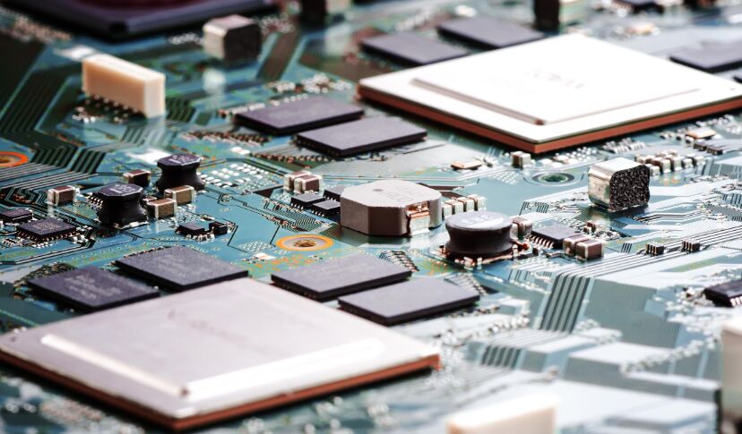
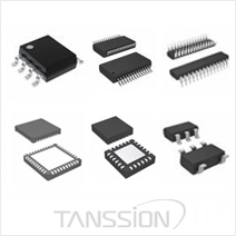
Semiconductors are used in integrated circuits, consumer electronics, communication systems, photovoltaic power generation, lighting, high-power power conversion and other fields. For example, diodes are devices made of semiconductors.


Common semiconductor materials include silicon, germanium, gallium arsenide, etc., and silicon is the most influential one in the application of various semiconductor materials. Semiconductor devices have replaced vacuum tubes in most applications. They use electrically conductive solid state rather than gaseous or thermionic emission in a vacuum.


A semiconductor is a material whose electrical conductivity is between that of a conductor and an insulator at room temperature. A semiconductor is a material with controllable conductivity, ranging from an insulator to a conductor. From the perspective of science and technology and economic development, semiconductors affect people's daily work and life. It was not until the 1930s that this material was recognized by the academic community.


Matter exists in various forms, such as solid, liquid, gas, plasma and so on. We usually call materials with poor conductivity, such as coal, artificial crystals, amber, ceramics, etc., as insulators. Metals with better conductivity, such as gold, silver, copper, iron, tin, aluminum, etc., are called conductors. Materials between conductors and insulators can simply be called semiconductors. Compared with conductors and insulators, the discovery of semiconductor materials is the latest. It was not until the 1930s, when the purification technology of materials was improved, that the existence of semiconductors was truly recognized by the academic community.


Ⅰ. History of semiconductor development


In 1833, Faraday, the father of electronics, a British scientist, first discovered that the resistance of silver sulfide varies with temperature differently than that of ordinary metals. In general, the resistance of metals increases with temperature, but Faraday discovered that the resistance of silver sulfide materials It decreases with the increase of temperature. This is the first discovery of the semiconductor phenomenon.


Soon, in 1839, Berclair of France discovered that the junction formed by the contact between the semiconductor and the electrolyte would generate a voltage under light, which was later known as the photovoltaic effect, which is the second characteristic of the discovered semiconductor.


In 1873, Smith of the United Kingdom discovered the photoconductive effect of selenium crystal material with increased conductance under light, which is the third characteristic of semiconductors.


In 1874, Braun of Germany observed that the conductance of some sulfides was related to the direction of the applied electric field, that is, its conduction had directionality, and it was turned on if a forward voltage was applied to both ends of it; If the polarity of the voltage is reversed, it will not conduct electricity. This is the rectification effect of the semiconductor, and it is also the fourth characteristic unique to the semiconductor.


Ⅱ. Band Structure of Semiconductors


The energy of electrons in semiconductors is limited to several energy bands between the ground state and free electrons. Inside the energy bands, the energy of the electrons is in a quasi-continuous state, while there is a gap between the energy bands. The electrons cannot in the band gap. When the electron is in the ground state, it is equivalent to the electron being bound near the nucleus; on the contrary, if the electron has the energy required by the free electron, it can completely leave the material.


Each energy band has several corresponding quantum states, and among these quantum states, the lower-energy ones have been filled with electrons. Of these quantum states that have been filled with electrons, the one with the highest energy is called the valence band. Under normal conditions in semiconductors and insulators, almost all electrons are in the valence band or the quantum state below it, so there are no free electrons to conduct electricity.

Common Semiconductor Types


The difference between semiconductors and insulators is that the width of the energy band gap between the two is different, that is, the minimum energy that electrons must obtain when they want to jump from the valence band to the conduction band is different. Generally, those with a bandgap width less than 3 electron volts (eV) are semiconductors, and those above are insulators.


At absolute zero, all electrons in a solid material are in the valence band, while the conduction band is completely empty. When the temperature starts to rise above absolute zero, some electrons may gain energy and enter the conduction band. The conduction band is the lowest energy band that allows electrons to move through the crystal and form a current after obtaining the energy of an external electric field, so the position of the conduction band is immediately above the valence band, and the gap between the conduction band and the valence band The gap is the energy band gap.


In the conduction band, the electrons associated with the formation of electric current are usually called free electrons. According to the Pauli exclusion principle, there cannot be two electrons in the same quantum state, so at absolute zero, the energy bands below the Fermi level, including the valence band, are all filled. Since the number of electrons with momentum in the opposite direction is equal in the filled energy band, it cannot carry current macroscopically.


Electrons in the valence band gain energy to jump to the conduction band, which leaves a vacancy in the valence band, a so-called hole. Both the electrons in the conduction band and the holes in the valence band contribute to the current transmission. The hole itself will not move, but other electrons can move to the hole, which is equivalent to the hole itself moving in the opposite direction. Holes are positively charged relative to negatively charged electrons.


A significant difference between semiconductors and conductors is that the current conduction of semiconductors comes from the contribution of both electrons and holes, while the Fermi level of conductors is already in the conduction band, so electrons do not need a lot of energy to find vacancies The quantum state for it to jump and cause electric current conduction.


The energy distribution of electrons within a solid material follows a Fermi-Dirac distribution. At absolute zero, the highest energy of electrons in the material is the Fermi level. When the temperature is higher than absolute zero, the Fermi level is the energy level with a probability of being occupied by electrons equal to 0.5 among all energy levels. The energy distribution of electrons in a semiconductor material is a function of temperature, which also makes its conductivity greatly affected by temperature. When the temperature is very low, there are fewer electrons that can jump to the conduction band, so the conductivity will also become poor.


Ⅲ. Semiconductor device materials


Silicon (Si) is by far the most widely used material in semiconductor devices. Its low raw material cost, relatively simple process, and useful temperature range make it the best compromise among competing materials. Silicon used in the manufacture of semiconductor devices is currently manufactured into boules of diameters large enough to allow the production of 300mm (12in) wafers.

Ge was a widely used early semiconductor material, but its thermal sensitivity made it less useful than silicon. Today, germanium is often alloyed with silicon for use in ultra-high-speed SiGe devices.

GaAs is also widely used in high-speed devices, but until now it has been difficult to form large-diameter blobs of this material, limiting wafer diameters to sizes significantly smaller than silicon wafers, enabling mass production of GaAs devices than Silicon is much more expensive.

SiC has found some applications as a raw material for blue light-emitting diodes (LEDs) and is being investigated for use in semiconductor devices that can withstand high operating temperatures and environments with high levels of ionizing radiation. IMPATT diodes have also been made from SiC.

Various indium compounds (indium arsenide, indium antimonide, and indium phosphide) are also being used in LEDs and solid-state laser diodes. Selenium sulfide is being studied in the manufacture of photovoltaic solar cells.


Ⅳ. Common semiconductors

1. Two-terminal devices: Schottky diodes, laser diodes, IMPATT diodes, PIN diodes, PIN diodes, Zener diodes, solar cells, light-emitting diodes (LEDs), etc.

2. Three-terminal devices: bipolar transistors, unijunction transistors, field effect transistors, Darlington transistors, insulated gate bipolar transistors, etc.

3. Four-terminal device: Hall effect sensor (magnetic field sensor), optocoupler

Common Semiconductor Types

Ⅴ. Semiconductor device application


All transistor types can be used as building blocks of logic gates, which are the basis of digital circuit design. In digital circuits such as microprocessors, transistors act as on-off switches. For example, in a MOSFET, the voltage applied to the gate determines whether the switch is on or off.

Transistors used in analog circuits cannot be used as on-off switches; instead, they respond to a continuous range of inputs with a continuous range of outputs. Common analog circuits include amplifiers and oscillators.

Circuits that interface or convert between digital and analog circuits are called mixed signal circuits.


Ⅵ. Classification and performance of semiconductors

1. Amorphous semiconductor

Also known as amorphous semiconductor or glass semiconductor, it belongs to a class of semiconductive materials. Amorphous semiconductors, like other amorphous materials, have short-range order and long-range disorder structures.

It mainly forms amorphous silicon by changing the relative position of atoms and changing the original periodic arrangement. The main difference between crystalline and amorphous states is whether the arrangement of atoms has a long order.

It is difficult to control the performance of amorphous semiconductors. With the invention of technology, amorphous semiconductors have begun to be used. This production process is simple and is mainly used in engineering. It has a good effect on light absorption and is mainly used in solar cells and liquid crystal displays.

2. Elemental semiconductors

Elemental semiconductors refer to semiconductors composed of a single element, among which silicon and selenium were studied earlier. It is a solid material composed of the same elements with semiconducting properties, which is easily changed by trace impurities and external conditions.

At present, only silicon and germanium have good performance and are widely used. Selenium is used in the fields of electronic lighting and optoelectronics. Silicon is widely used in the semiconductor industry, which is mainly affected by silicon dioxide, which can form a mask in device manufacturing, improve the stability of semiconductor devices, and facilitate automated industrial production.

3. Intrinsic semiconductor

A semiconductor that does not contain impurities and has no lattice defects is called an intrinsic semiconductor. At extremely low temperatures, the valence band of a semiconductor is full. After thermal excitation, some electrons in the valence band will cross the forbidden band and enter the empty band with higher energy. After electrons exist in the empty band, they will become the conduction band. The absence of an electron creates a positively charged vacancy, called a hole.

Hole conduction is not actual motion, but an equivalence. When electrons conduct electricity, holes with equal charge will move in the opposite direction. They produce directional movement under the action of an external electric field to form a macroscopic current, which are called electron conduction and hole conduction respectively. This mixed conduction due to the generation of electron-hole pairs is called intrinsic conduction.

At a certain temperature, the generation and recombination of electron-hole pairs exist at the same time and reach a dynamic equilibrium. At this time, the semiconductor has a certain carrier density and thus a certain resistivity. When the temperature rises, more electron-hole pairs will be generated, the carrier density will increase, and the resistivity will decrease. Pure semiconductors without lattice defects have a relatively large resistivity, and there are not many practical applications.

4. Inorganic composite semiconductor

Inorganic composites are mainly composed of a single element to form a semiconductor material. Of course, there are also semiconductor materials composed of multiple elements. The main semiconductor properties are Group I and Group V, VI, VII; Group II and Group IV, V, VI, VII; III Combination compounds of group V and VI; group IV and IV and VI; group V and VI; group VI and group VI.

This semiconductor is mainly used in high-speed devices. The speed of transistors made by InP is higher than that of other materials, and it is mainly used in optoelectronic integrated circuits and anti-nuclear radiation devices. For materials with high conductivity, it is mainly used in LED and other aspects.

5. Organic synthetic semiconductors

Organic compounds refer to compounds containing carbon bonds in the molecule. The organic compound and the carbon bond are vertically superimposed to form a conduction band. Through chemical addition, it can be allowed to enter the energy band, so that conductivity can occur, thereby forming organic compound semiconductors.

Compared with previous semiconductors, this semiconductor has the characteristics of low cost, good solubility, and easy processing of light materials. The conductivity can be controlled by controlling the molecules, and the application range is relatively wide, mainly used in organic thin films, organic lighting, etc.


Ⅶ. Doping of Semiconductors


The reason why semiconductors are widely used in today's digital world is that they can change the characteristics of essential semiconductors by adding impurities to them. This process is called doping. The concentration and polarity of impurities doped into the intrinsic semiconductor will have a great impact on the conductivity of the semiconductor. The doped semiconductor is called impurity semiconductor.

Dopants are classified into donors and acceptors according to the positive and negative charges they bring to the doped material. Most of the valence electrons brought by the donor atoms will form covalent bonds with the doped material atoms, and then be bound. The electrons that are not covalently bonded to the doped material atoms are weakly bound by the donor atoms and are called donor electrons.

Compared with the valence electrons of intrinsic semiconductors, the energy required for donor electrons to transition to the conduction band is lower, and it is easier to move in the crystal lattice of semiconductor materials and generate current. Although the donor electron gains energy and jumps to the conduction band, it does not leave a hole like the intrinsic semiconductor, and the donor atom will only be fixed in the crystal lattice of the semiconductor material after losing the electron. Therefore, this semiconductor that obtains excess electrons to provide conduction due to doping is called an n-type semiconductor, and n represents negatively charged electrons.

Contrary to the donor, when the acceptor atom enters the semiconductor lattice, because its number of valence electrons is less than that of the semiconductor atom, it will equivalently bring a vacancy, and this extra vacancy can be regarded as a hole. Acceptor-doped semiconductors are called p-type semiconductors, where p represents positively charged holes.

The effect of doping is illustrated with an intrinsic semiconductor of silicon. Silicon has four valence electrons, and the dopants commonly used in silicon include trivalent and pentavalent elements. When a trivalent element with only three valence electrons, such as boron, is doped into a silicon semiconductor, boron acts as an acceptor, and the boron-doped silicon semiconductor is a p-type semiconductor. Conversely, if a pentavalent element such as phosphorus is doped into a silicon semiconductor, the phosphorus acts as a donor, and the phosphorus-doped silicon semiconductor becomes an n-type semiconductor.


Ⅷ. Semiconductor Refrigeration Technology


Semiconductor refrigeration technology is a method of refrigeration using the characteristics of semiconductor materials, and it has been widely used in some specific applications. This technology typically uses semiconducting materials called thermoelectric materials, which generate heat and cold when an electric current passes through them.

Semiconductor refrigeration technology can effectively control the ambient temperature, especially for some plants that have high requirements on the environment. Using semiconductor refrigeration technology to shape the growth environment can promote the growth of plants.

1. Operating principle

The application principle of semiconductor refrigeration technology is based on the Peltier principle. In 1834, French scientist Peltier discovered semiconductor refrigeration. The Peltier principle is also known as the "Peltier effect", which is to make full use of two different conductors, use a circuit composed of A and B, and connect direct current, and Joule heat can be generated at the joint of the circuit, and at the same time Some other heat will also be released. At this time, it will be found that the other joint is not releasing heat, but absorbing heat.

This phenomenon is reversible. As long as the direction of the current is changed, the exothermic and endothermic operations can be adjusted. There is a proportional relationship between the intensity of the current and the heat absorbed and released, which is consistent with the semiconductor itself. Nature is also related. Since the Peltier effect of metal materials is relatively weak, and semiconductor materials operate on the Peltier principle, the effect produced will be stronger.

2. Application strategy

Semiconductor refrigeration technology has been widely used in the field of medicine, industry, and even in daily life. For example, the use of conductor refrigeration technology in various modern refrigeration equipment, such as refrigerators, air conditioners, etc., can be equipped with electronic coolers. Semiconductor refrigerators use semiconductor refrigeration technology.

Common Semiconductor Types

Different numbers of semiconductor cooling chips can be connected in parallel or in series according to the needs during the connection process, and they can play a role when they are placed in a suitable position. In the 1950s, the former Soviet Union developed a small model refrigerator with a capacity of only 10 liters. The refrigerator is very small and easy to use. Japan has developed a refrigerator that is specially used to store red wine. The temperature must be strictly controlled, and the application of semiconductor refrigeration technology can meet the refrigeration requirements of the refrigerator. With the continuous development of society, people have higher and higher requirements for refrigeration equipment while pursuing the quality of life.

The use of semiconductor air conditioners is different from the air conditioners used in daily life, but is used in special places, such as engine rooms, submarines and so on. The use of relatively stable refrigeration technology can not only ensure rapid refrigeration, but also meet the requirements of semiconductor refrigeration technology.


Tags:

Frequently Asked Questions

1、What is the difference between a semiconductor and a conductor and an insulator?
Conductors are a class of materials with high electrical conductivity, allowing electrons to flow freely. Insulators are a class of materials with extremely low electrical conductivity, making it difficult for electrons to move through them. Semiconductors are between conductors and insulators, and their electrical conductivity is in between.
2、What is photolithography in semiconductor process?
Photolithography is a critical step in semiconductor processing, used to create tiny patterns and structures on the surface of silicon wafers (or other semiconductor materials).
3、What is the role of PN junction in semiconductor devices?
The PN junction is the basic structure of a diode. In the PN junction, due to the different material properties between the P region and the N region, a potential difference is formed; the PN junction is a structure between the base (B) and the emitter (E) in the transistor. In NPN transistors, the PN junction is between the base and emitter.

Leave a Comment

Related Articles

Popular Parts

#10FWZ

#10FWZ

#292KNAS-T1028Z

#292KNAS-T1028Z

#458PT-1566=P3

#458PT-1566=P3

#458PT-1720=P3

#458PT-1720=P3

#458PT-2002=P3

#458PT-2002=P3

#458PT-2078=P3

#458PT-2078=P3

#617PT-2038=P3

#617PT-2038=P3

#617PT-2270=P3

#617PT-2270=P3

Popular Tags

PMIC Audio Products Logic Interface capacitors linear controllers embedded Line Protection drivers amplifiers Distribution Backups wireless modules memory converters Battery Products sensors filters relays Switches distribution analog Clock timing voltage diodes speakers Batteries Rechargeable battery regulators Fiber Optic Cables Cable Assemblies routers microcontroller Backups audio Magnetics - Transformer Inductor Components cables Electric Double Layer Capacitors (EDLC) Supercapa inductors transformer optoelectronics potentiometer resistors switching management special digital purpose signal Discrete Semiconductor Ceramic Capacitors semiconductor cable Alarms equipment resonators oscillators crystals kits accessories isolators motors RF Transformers monitors comparators specialized programmable microcontrollers FPGAs Data Acquisition application specific gates inverters Buffers Transceivers dividers Sensor decoders microprocessors microprocessor DC video circuit protection microphones PCB Integrated Circuits (ICs) PMIC - Lighting Memory Cards SSDs HDDs Wires Tantalum Capacitors Transducers LEDs Battery Chargers 4G Ballast Controllers Vacuum Tubes Transistors - Bipolar (BJT) - Single counter integrated circuits Guitar Parts Buzzer Elements transducers circuit Computer Equipment Piezo Benders boxes Magnetics enclosures racks Buzzers wires and Sirens wire Buzzers and Sirens inductor components connectors interconnects CR2450 LR44 Embedded Computers TXS0108EPWR fans SS14 thermal UA741CP RC4558P hardware TNY268PN fasteners MJE2955T UC3842AN TOP245YN coils SN6505BDBVR chokes BD139 controls ATMEGA328-PU automation NE5532P identification barriers signs labels protection inductor educational networking resistor powersupply power supply prototyping fabrication desoldering soldering ESD static Tapes adhesives materials Test measurement Tools Uncategorized Specialized ICs voltage Regulators contro thermal Management motor laser full half switchers batteries translators shift latches flip flops voice playback serializers deserializers active synthesis PLDs clocks delay lines reference supervisors PoE correction lighting ballast hot swap energy metering specialty parity generators checkers FIFOs multipliers instrumentation UARTs terminators capacitive touch Modems ICs Encoders DSP Data acquisition front end timers synthesizers frequency regulator controller regula RMS power OR ideal LED gate display chargers configuration proms universal bus functions multiplexers multivibrators counters processing amps telecom repeaters splitters detector interfaces I/O expanders receivers CODECs system SoC CPLDs Complex amplifier IF RFID Oscillator Externally excited oscillator fuses switchs transistors shunt thyristor Oscillators Resonators Ballast Controllers Coils Chokes RF Filters RF/IF and RFID RF Amplifiers Battery Packs SAW Filters Mica and PTFE Capacitors Accessories Piezo Benders 1 222 sdsd ballasts starter SSD HDD Modules

Popular Posts