Ⅰ. What is an operational amplifier?
Ⅱ. The development of operational amplifiers
Ⅲ. Principle of operational amplifiers
Ⅳ. Operational amplifier parameters
Ⅴ. How is the random noise of the operational amplifier generated?
Ⅵ. Why do operational amplifier circuits generally adopt the inverting input mode?
It has been decades since the invention of the operational amplifier. From the earliest vacuum tube to today's integrated circuit, it has always played a pivotal role in different electronic products. And the rise of emerging applications such as information appliances, mobile phones, PDAs, and networks has pushed operational amplifiers to a new level.
Ⅰ. What is an operational amplifier?
Because of its early application in analog computers to realize mathematical operations, it was named "operational amplifier". It is an amplifier with a special coupling circuit and feedback. Its output signal can be the result of mathematical operations such as addition, subtraction, or differentiation and integration of the input signal. An operational amplifier is a circuit unit named from a functional point of view, which can be realized by a discrete device or in a semiconductor chip.
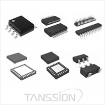
An operational amplifier is a circuit unit with a certain magnification, usually combined with an external feedback network to form a functional module, such as a buffer, a proportional amplifier, an adder, an integrator, etc. Take Awinic's operational amplifier AWS90001 as an example. It is a single-channel low-voltage, low-power, rail-to-rail operational amplifier with five PIN pins, as shown in the figure below. Among them, IN+ and IN- are the non-inverting input terminal and the inverting input terminal respectively, V+ and V- are the power supply of the operational amplifier, and OUT is the output.

Ⅱ. The development of operational amplifiers
1941: Vacuum tube operational amplifier. Karl D. Swartzel Jr. of Bell Laboratories invented the first operational amplifier composed of vacuum tubes and named it "Summing Amplifier".
1949: Chopper-stabilized operational amplifier. In 1949, Edwin A. Goldberg designed the chopper-stabilized operational amplifier.
1952: Commercial operational amplifiers are introduced. The first operational amplifier sold as a commercial product was the George A. Philbrick Researches (GAP/R) vacuum tube operational amplifier, model K2-W.
1963: The monolithic IC operational amplifier is introduced. The first operational amplifier to be made in the form of a single integrated circuit chip was the μA702 designed by Bob Widlar of Fairchild Semiconductors. In 1965 it was improved and introduced the μA709.
1968: μ A741 released. Fairchild Semiconductor Company Launches μ A741. It is still in production and use to date, making it the most successful operational amplifier in history and one of the few IC models with the longest lifespan.
Ⅲ. Principle of operational amplifiers
The operational amplifier has a signal output port (Out) and two high-impedance input ports, non-inverting and inverting. In order to distinguish, the reverse input terminal and the non-inverting input terminal are marked with "-" and "+" respectively.

There are two types of power supply for operational amplifiers: dual-supply and single-supply. For a dual-supply operational amplifier, its output can vary on either side of zero voltage. Based on the input signal, it can output both positive and negative signals. A single-supply operational amplifier whose output varies between power and ground.

Ⅳ. Operational amplifier parameters
1. Slew Rate
It indicates the degree to which the operational amplifier can track the change speed of the input signal, and the unit is V/us.
2. Input Offset Current
When the output DC voltage of the operational amplifier is zero, the difference between the bias currents of the two input terminals. The input offset current also reflects the circuit symmetry inside the op amp. The better the symmetry, the smaller the input offset current. The input offset current is approximately one hundredth to one tenth of the input bias current. The input offset current has an important influence on small signal precision amplification or DC amplification, especially when a larger resistor is used outside the operational amplifier. Input offset current can affect accuracy more than input offset voltage can. The smaller the input offset current, the smaller the intermediate zero offset during DC amplification, and the easier it is to handle. Therefore, the input offset current is an extremely important indicator for precision operational amplifiers.
3. Input Offset Voltage Drift
It is also called the temperature coefficient TC VOS, generally a few uV/.C. It represents the ratio of the change in input offset voltage to the change in temperature within a given temperature range. This parameter is actually a supplement to the input offset voltage, which is convenient for calculating the drift of the amplifier circuit due to temperature changes within a given operating range. The temperature drift of the input offset voltage of the general operational amplifier is between ±10~20μV/℃, while the temperature drift of the input offset voltage of the precision operational amplifier is less than ±1μV/℃.
4. Input Resistance
It represents the differential input resistance between the two input terminals of the operational amplifier. This value is defined by a tiny AC signal, and the actual influence is so small that it can be ignored. The common-mode input resistance at the input of the operational amplifier is 10-1000 times that of Rin, which is also negligible.
5. Maximum Output Voltage
The output voltage before saturation is called the maximum output voltage. An ideal op amp achieves rail-to-rail output.
6. Input Bias Current
When the output DC voltage of the operational amplifier is zero, the average value of the bias current at its two input terminals. The input bias current has a greater impact on the places where the input impedance is required, such as high-impedance signal amplification and integration circuits. The input bias current has a certain relationship with the manufacturing process. The input bias current of the bipolar process (that is, the above-mentioned standard silicon process) is between ±10nA~1μA. The input bias current of the input stage using FETs is generally lower than 1nA.
7. Current Consumption
This current refers to the current flowing through the power supply terminal of the operational amplifier, which varies with the external circuit and power supply voltage. When the operational amplifier is connected into a closed-loop condition, a large signal (including a step signal) is input to the input terminal of the operational amplifier, and the output rising rate of the operational amplifier is measured from its output terminal. Since the op amp's input stage is switched during conversion, its feedback loop has no effect, that is, the slew rate is independent of the closed-loop gain. The slew rate is a very important indicator for large signal processing. For general operational amplifiers, the slew rate SR<=10V/μs, and for high-speed op amps, the slew rate SR>10V/μs. The highest slew rate SR of current high-speed operational amplifiers reaches 6000V/μs, which is used in the selection of operational amplifiers in large signal processing.
8. Input Offset Voltage
The compensation voltage applied between the two input terminals when the output terminal voltage of the integrated operational amplifier is zero. The input offset voltage actually reflects the symmetry of the circuit inside the op amp, the better the symmetry, the smaller the input offset voltage. The input offset voltage is a very important indicator of an op amp, especially when it is a precision op amp or used for DC amplification. The input offset voltage has a certain relationship with the manufacturing process, and the input offset voltage of the bipolar process (that is, the above-mentioned standard silicon process) is between ±1~10mV; if the field effect transistor is used as the input stage, the input offset voltage will be larger Some. For precision op amps, the input offset voltage is generally below 1mV. The smaller the input offset voltage, the smaller the intermediate zero offset during DC amplification, and the easier it is to handle. Therefore, it is an extremely important indicator for precision op amps.
If both inputs of the op amp are grounded, the output of the ideal op amp is zero, but the output of the real op amp is not zero. At this time, the equivalent input voltage obtained by dividing the output voltage by the gain is called the input offset voltage, and its value is several mV. The smaller the value, the better. When the value is larger, the gain is limited.
9. Gain Bandwidth Product
Under the condition that the closed-loop gain of the operational amplifier is 1 times, a small constant-amplitude sine signal is input to the input terminal of the operational amplifier, and the signal frequency corresponding to the 3db drop of the closed-loop voltage gain is measured from the output terminal of the operational amplifier. Unity gain bandwidth is a very important specification. For sinusoidal small-signal amplification, the unity-gain bandwidth is equal to the product of the input signal frequency and the maximum gain at that frequency. This is used in the selection of operational amplifiers in small signal processing.
10. Voltage Gain
It is also called differential voltage gain. The voltage gain of an ideal operational amplifier is infinite, and the actual operational amplifier is generally about several hundred dB. It represents the ratio of the output voltage of the operational amplifier to the input voltage of the differential mode voltage when the operational amplifier is operating in the linear region. Because the differential-mode open-loop DC voltage gain is very large, the differential-mode open-loop DC voltage gain of most operational amplifiers is generally tens of thousands of times or more. Because it is inconvenient to directly express by numerical value, we generally use the decibel method to record and compare. The differential-mode open-loop DC voltage gain of a general operational amplifier is between 80 and 120dB, while the differential-mode open-loop voltage gain of an actual operational amplifier is a function of frequency. For the convenience of comparison, we generally use the differential-mode open-loop DC voltage gain.
11. Input Common-Mode Voltage Range
It represents the range of common-mode voltage that can be applied between the two input terminals of the operational amplifier and the ground. A full-scale output op amp approaches this characteristic when the common-mode input voltage range is equal to the positive and negative supply voltages.
12. Supply Voltage Rejection Ratio
When the op amp works in the linear region, the ratio of the input offset voltage of the op amp to the power supply voltage. The supply voltage rejection ratio reflects the impact of power supply changes on the output of the op amp. At present, the power supply voltage rejection ratio can only be about 80dB. Therefore, when used for DC signal processing or small signal processing analog amplification, the power supply of the operational amplifier needs to be carefully processed. Of course, an op amp with a high common-mode rejection ratio can compensate for some of the supply-voltage rejection ratio. In addition, when using dual power supplies, the power supply voltage rejection ratios of the positive and negative power supplies may be different.
As the positive and negative supply voltages change, that change appears at the output of the op amp and is scaled to the value at the op amp's input. If the equivalent input conversion voltage is ΔVin when the power supply changes ΔVs, then SVRR is defined as:
SVRR = ΔVs/ΔVin
Ⅴ. How is the random noise of the operational amplifier generated?
The noise that appears at the output of an op amp is measured in terms of voltage noise. But both voltage noise sources and current noise sources can generate noise. All internal noise sources of an operational amplifier are usually referred to the input, that is, as uncorrelated or independent random noise generators connected in series or in parallel with the two inputs of an ideal noise-free amplifier. We consider op amp noise to have three basic sources:
1. A noise voltage generator (similar to offset voltage, usually in series with the non-inverting input).
2. Two noise current generators (similar to bias currents, sink current through two differential inputs).
3. Resistor Noise Generators (If there are any resistors in the op-amp circuit, they will also generate noise. We can think of this noise as coming from a current source or a voltage source. Either form is common to us in a given circuit . )
The voltage noise of the op amp can be as low as 3 nV/Hz. Voltage noise is a technical indicator that is usually emphasized. But it is often the limiting factor in system noise performance at high impedances. This condition is similar to a disorder. Offset voltage is often responsible for output offset, but bias current has the real responsibility. Bipolar op amps have lower voltage noise than traditional FET op amps. Despite this advantage, the current noise is still relatively large in practice. Today's FET op amps achieve the voltage noise levels of bipolar op amps while maintaining low current noise.

Ⅵ. Why do operational amplifier circuits generally adopt the inverting input mode?
1. The major difference between the inverting input method and the non-inverting input method is:
In the inverting input method, a balanced resistor is connected to the ground at the non-inverting terminal, and there is no current on this resistor (because the input resistance of the operational amplifier is extremely large), so the non-inverting terminal is approximately equal to the ground potential, which is called "virtual ground". The potentials of the inverting terminal and the non-inverting terminal are very close, so there is also a "virtual ground" at the inverting terminal. The advantage of having a virtual ground is that there is no common-mode input signal. Even if the common-mode rejection ratio of this op amp is not high, there is guaranteed to be no common-mode output. However, there is no "virtual ground" in the non-inverting input connection. Common-mode input signals are created when single-ended input signals are used. Even with an op amp with a high common-mode rejection ratio, there will still be a common-mode output. Therefore, in general, we will try our best to use the inverting input connection method when using it.
2. The positive phase is the oscillator, and the negative phase can stabilize the amplifier, and access to negative feedback.
3. From a principle point of view, it is possible to connect to a proportional amplifier circuit of the same phase. However, in practical applications, the amplified signal (that is, the differential mode signal) is often very small. At this time, we must pay attention to suppressing noise (usually expressed as a common mode signal). However, the same-phase proportional amplifier circuit has a poor ability to suppress common-mode signals, and the signal to be amplified will be submerged in noise, which is not conducive to post-processing. Therefore, we generally choose an inverse proportional amplifier circuit with better suppression ability.
Tags:Sensors Transducers Amplifiers